
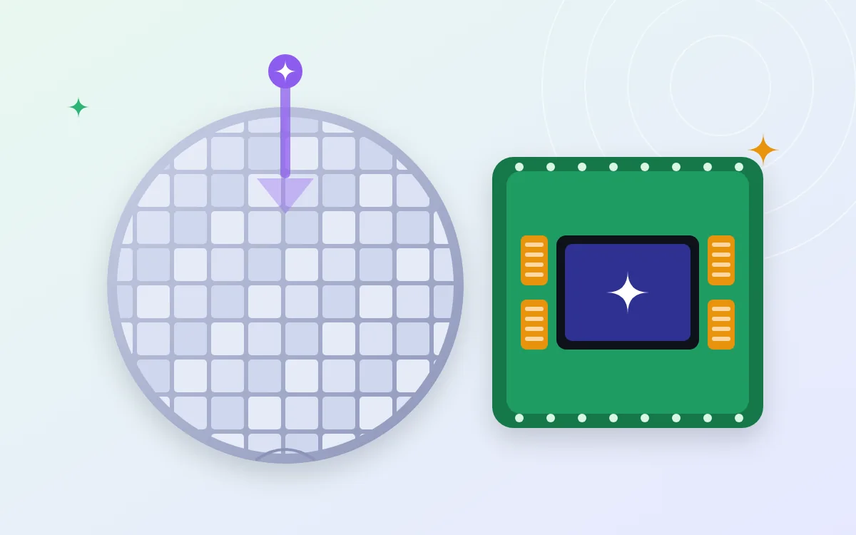
Nvidia designs some of the most advanced chips in the world, but it does not own the factories that make them. Its chips are designed in California, manufactured mostly by TSMC, combined with memory from other specialists, and then built into servers. This guide explains that journey in plain language, using Nvidia's Blackwell generation as the example.
It is written by a software team, not chip engineers, so we stay with how the process works and what it means for the cloud services developers in Nepal rent. Sources are listed at the end.
The short version
- Design: engineers describe the chip in code and test it virtually before anything is built.
- Wafers: ultra-pure silicon is grown into a crystal and sliced into thin discs.
- Fabrication: the circuits are built up layer by layer on each wafer, using light patterns, etching and deposition.
- Testing and cutting: every chip on the wafer is tested, then cut out.
- Packaging: the processor is joined to stacked high-bandwidth memory on a silicon base.
- Systems: finished modules go onto boards, into servers and into racks in data centres.
Step 0: Nvidia designs, partners build
Nvidia is a 'fabless' company: it uses outside suppliers for every stage of manufacturing, and TSMC is its primary manufacturing partner. Designing a chip means defining its architecture, describing it in a hardware description language, simulating it, laying out billions of transistors and checking that the result will work.
The end of that work is called the tape-out: the final design is turned into the set of masks used to print the chip. After that, changes are slow and expensive, which is why so much testing happens first.
Step 1: From sand to wafers
Chips are made on silicon, which comes from sand. It is purified to an extreme degree, melted and grown into a single large crystal, then sliced into thin round wafers and polished until almost perfectly flat. Modern chip factories use wafers 300 millimetres across.
Size matters here. A large data-centre processor means only a few dozen chips fit on one wafer, and every one that is lost to a defect is a large share of the wafer's value.
Step 2: Fabrication, one layer at a time
Fabrication takes place in a cleanroom, in a long loop of repeating steps. A thin film is deposited, the wafer is coated with a light-sensitive layer called photoresist, light projects the chip's pattern onto it, the exposed areas are developed away, and the film beneath is etched or treated with other atoms. Then the cycle repeats for the next layer. The lowest layers form the transistors, and the upper layers are metal wiring that connects them.
The step that decides how small the features can be is lithography. For the finest layers the industry uses extreme ultraviolet (EUV) light with a wavelength of about 13.5 nanometres. It is produced by firing tiny droplets of molten tin through a vacuum chamber and hitting each one with a laser, which turns it into a plasma that emits EUV light. Because glass and air absorb EUV, the light is steered by mirrors in a vacuum rather than lenses. As of 2025, ASML is the only company that sells EUV machines for chip production.
Step 3: Two big dies, one GPU
Nvidia says its Blackwell GPUs pack 208 billion transistors and are made on a custom TSMC process called 4NP. Every Blackwell product has two reticle-limited dies combined into one GPU. The reticle limit is the largest area the lithography machine can print in one exposure, so it caps how big a single die can be.
Nvidia's answer is to make two dies close to that maximum size and join them with a 10 terabytes-per-second chip-to-chip link, so that software sees them as one processor.
Step 4: Testing, sorting and cutting
Before the wafer is cut, every chip on it is probed with electrical tests. Defects are unavoidable at these scales, and a larger chip has a higher chance of containing one, which is why yield, the share of working chips, matters so much to cost. The chips that pass are cut out of the wafer.
In general, chipmakers also sort finished parts by how well they perform, a practice called binning, so that the same underlying design can be sold in more than one tier.
Step 5: Advanced packaging with stacked memory
An AI chip is only as fast as the data it can reach, so the GPU is not used on its own. It is joined to high-bandwidth memory (HBM), which stacks several memory dies on top of each other, linked vertically by tiny channels called through-silicon vias. The memory stacks sit right beside the processor on a thin silicon base called an interposer, which carries a very large number of short, fast connections between them.
TSMC's version of this packaging is called CoWoS. The three largest HBM makers are SK Hynix, Samsung and Micron, so a single AI processor depends on several companies working together.
Step 6: From chip to server
The packaged processors are tested again, mounted on modules and boards, and built into servers and racks with fast networking and cooling. Most of them are never seen by the people who use them. They sit in data centres run by cloud providers, who rent the computing power out by the hour.
Why this matters
- Few places do the hardest steps. Leading-edge lithography and advanced packaging are concentrated in a small number of companies, so supply is slow to expand and easy to disrupt.
- Memory is half the story. Stacked memory and the packaging that connects it matter as much to AI performance as the processor does.
- Software multiplies the hardware. A chip is only useful with the drivers, libraries and frameworks that let developers program it, and that software is a large part of why these chips are so widely used.
What it means for developers in Nepal
Almost nobody building AI software in Nepal needs to buy these chips. You rent them: cloud providers offer GPU servers by the hour, and model providers offer AI through APIs. The practical questions are the ones in our other guides: whether a task needs AI at all, what each use costs, where your data is processed and how you test the result.
See adding AI to business software in Nepal and AI engineering in Nepal: skills and roadmap. For the longer history that led to these chips, read From Abacus to AI.
Next steps
If you are planning an AI feature and want help choosing between renting GPUs, calling a model API or not using AI at all, talk to our team.
Sources and further reading
- NVIDIA: Blackwell architecture
- Wikipedia: Nvidia
- Wikipedia: Extreme ultraviolet lithography
- Wikipedia: High Bandwidth Memory
Have a project in mind?
Tell us what you're trying to solve. Or keep reading: SEO for AI Search: What Google Says Still Works.